E-Ink Weather Station
March 2026 – Present · Rev B.2 frozen August 2026 · Source on GitHub
Overview
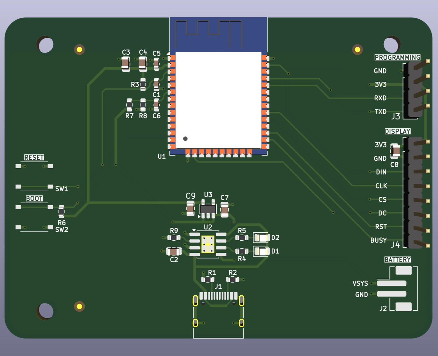
A battery powered 2-layer ESP32-WROOM-32 board that pulls weather data over WiFi and displays it on a Waveshare 4.2 inch four-color e-paper panel. USB-C feeds a TP4056 lithium charger, the cell feeds an AP2112K-3.3 regulator, and the ESP32 sleeps between hourly updates.
The design went through two revisions. Rev A was fully routed and looked finished, but it would not have run on a battery. Rev B.2 is 80 × 60 mm with 35 components, 52 nets, and 49 vias, fully routed with no DFM violations at JLCPCB's standard tier.
Regulator Selection
Rev A used an AMS1117-3.3, which has about 1.1 V of typical dropout and draws roughly 5 mA quiescent. A single lithium cell runs from 4.2 V down to 3.0 V, so after dropout the 3.3 V rail would have sat near 2.9 V on a full charge and fallen further as the cell drained, below the ESP32 minimum of 3.0 V. The quiescent draw was a second problem on its own, since 5 mA flattens a 2000 mAh cell in about two weeks with the board doing nothing.
Rev B replaced it with an AP2112K-3.3 in SOT-23-5, rated at 250 mV typical dropout at 600 mA and 55 µA quiescent. Cutting dropout from 1.1 V to 250 mV is what makes battery operation possible at all.
One consequence is worth recording. The AP2112K drops out around 3.55 V while the battery pack's protection circuit does not cut off until 2.4 to 3.0 V, so the ESP32 browns out well before protection ever engages. Usable capacity is therefore about 85% of the cell rather than all of it.
Antenna Keep-Out
In Rev A the ESP32 module sat mid-board with its antenna pointing inward. The footprint keep-out carved a 48 × 21 mm strip of bare FR4 through the middle of the board, about 37% of the total area, and stranded the display header on the far side of it. Six SPI signals and two ground stitching traces ran directly through the antenna region to reach that header, which detunes the antenna and costs range.
Rev B moves the module to the board edge so the keep-out falls outside the board entirely, and relocates the display header. I verified the result against the raw board geometry rather than relying on DRC. Across the antenna window, copper is absent from the board edge down to the module's own pad row, with no tracks, vias, or foreign pads.
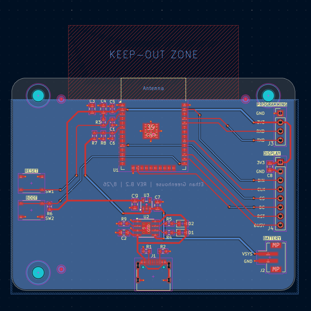
Rev B.2 layout. The hatched keep-out zone sits almost entirely off the board, which is the whole point of moving the module to the edge. Open it full size to zoom in.
Power Path
USB-C feeds a TP4056 charger set to 500 mA by a 2.4 kΩ program resistor, which is 0.25 C into the 2000 mAh pack. Both CC pins carry their own 5.1 kΩ pulldown.
System load sits on the same node as the charger's battery pin, which can corrupt charge termination because the TP4056 terminates when current falls to 50 mA. I planned a load sharing FET to fix this, then checked the duty cycle. The board is awake about 26 seconds per hour against a 100 µA baseline, roughly 500 times below the threshold, so termination works as built. The exception is bench development with USB connected and WiFi running continuously, which does exceed the threshold.
Battery voltage is sensed through a 1 M/1 M divider into IO34. That is an ADC1 channel, which matters because ADC2 is unusable while WiFi is active.
Estimated draw is about 11 mAh per day active and 2.4 mAh per day asleep, roughly 13 mAh per day total, which is about four months per charge. These are calculated from datasheet figures rather than measured, since the board has not been built. WiFi also has to be off before a panel refresh, because ESP32 transmit peaks near 500 mA against the regulator's 600 mA rating.
Manufacturing
The board sits inside JLCPCB's standard process at 0.25 mm minimum track, 0.416 mm minimum spacing, and 0.3 mm minimum drill. Two layers, all 27 SMD parts on the front for single sided assembly, two through hole connectors, fiducials present, zero violations.
The accepted tradeoff is grounding. 25 track segments route on the bottom layer and cut the ground pour, with the worst case at 28.6% reference coverage on the display chip select net. That is a radiated emissions concern rather than a functional one, and SPI to a slow e-paper panel will work fine. It would need addressing on a board seeking certification.
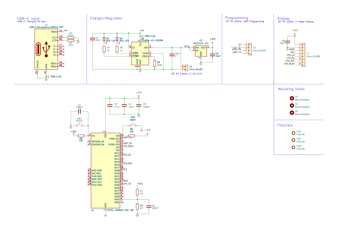
Full schematic. Open it full size to zoom in.
Status
Design frozen in August 2026 and cleared for fabrication, with gerbers, BOM, and pick and place files generated. The board has not been built yet.
The first step at bring-up is metering the battery connector polarity, since JST PH pigtails are not consistently wired and there is no reverse polarity protection on this board. After that, power from USB only and confirm 3.3 V at the display header before connecting the panel, measure sleep current against the estimate above, and isolate how much the display module's level translator draws, since it is permanently powered with no way to shut it off.